
Nanolithography is the branch of nanotechnology concerned with the study and application of the nanofabrication of nanometer-scale structures, meaning nanopatterning with at least one lateral dimension between the size of an individual atom and approximately 100 nm.
What is lithography used for?
Techniques - lithography Lithography, which is also called optical lithography or UV lithography, is a process used in microfabrication to pattern parts of a thin film or the bulk of a substrate. It uses light to transfer a geometric pattern from a photomask to a light-sensitive chemical "photoresist", or simply "resist," on the substrate.
What is nanoscale lithographic technology?
Modern lithographic equipment operates well inside the nanoscale regime, defined as features smaller than 100 nanometers (nm). The College of Nanoscale Science and Engineering (CNSE) is home to numerous systems of this caliber. The light bulb in Figure 1 is intentionally shown as blue.
What is the difference between lithography and nanolithography?
However, lithography is considered a hybrid approach, because the etching process is top-down, whereas the growth of nanolayers is bottom-up. Also, nanomanipulation, nanoimprint, and nanolithography are bottom-up approaches. Fig. 3.8.
What is the history of lithography in nanomaterials?
While lithographic techniques have been around since the late 18th century, none were applied to nanoscale structures until the mid-1950s. With evolution of the semiconductor industry, demand for techniques capable of producing micro- and nano-scale structures skyrocketed.
What is lithography and its types?
Lithography (from Ancient Greek λίθος, lithos 'stone', and γράφειν, graphein 'to write') is a planographic method of printing originally based on the immiscibility of oil and water. The printing is from a stone (lithographic limestone) or a metal plate with a smooth surface.
What is photolithography in micro and nanotechnology?
Photolithography is a nanotechnology procedure that creates micro-and nanoscale devices such as integrated circuits. It is the primary technique for producing integrated circuits and virtually everything else classified as “electronics.” The following are some examples of such electronic devices: computers.
What is nanolithography used for?
Nanolithography can be used for the development of well-defined 2D metal arrays on a substrate employing electron beam lithography (EBL), which is widely used to create metal nanostructures through scaling down the existing “parent-focus” layer via an electron beam (Hatzor and Weiss, 2001; Liu et al., 2011).
What is lithography in MEMS?
Lithography in the MEMS context is typically the transfer of a pattern to a photosensitive material by selective exposure to a radiation source such as light. A photosensitive material is a material that experiences a change in its physical properties when exposed to a radiation source.
What is the difference between lithography and photolithography?
Photolithography undergoes many steps in order to create one microfluidics device, whereas soft lithography uses a master mold created by photolithographic methods.
How is lithography done?
Lithography is a planographic printmaking process in which a design is drawn onto a flat stone (or prepared metal plate, usually zinc or aluminum) and affixed by means of a chemical reaction.
What are the types of nanolithography?
A typical commercial use of nanolithography is in the manufacture of semiconductor chips for computers.Nanolithography Techniques.Photolithography.Electron Beam Lithography (EBL)X-ray Lithography.Extreme Ultraviolet Lithography (EUVL)Light Coupling Nanolithography (LCM)Scanning Probe Microscope Lithography (SPM)More items...•
How does nanolithography work?
Generally, most nanolithography techniques make use of the properties of light or electrons to create patterns in a substrate. This patterning can be targeted via the use of masks being added to the photoresist in order to protect areas from the incoming light.
How does semiconductor lithography work?
A semiconductor lithography system undertakes a process whereby highly complex circuit patterns drawn on a photomask made of a large glass plate are reduced using ultra-high-performance lenses and exposed onto a silicon substrate known as a wafer.
What is photolithography process?
The photolithography process involves light exposure through a mask to project the image of a circuit, much like a negative image in standard photography. This process hardens a photo-resistive layer on the PCB or wafer. The hardened areas stay behind in the form of circuit paths of PCBs and CPUs.
What is the purpose of photoresist?
A photoresist (also known simply as a resist) is a light-sensitive material used in several processes, such as photolithography and photoengraving, to form a patterned coating on a surface. This process is crucial in the electronic industry.
What is the difference between positive and negative photoresist?
Positive photoresists are able to maintain their size and pattern as the photoresist developer solvent doesn't permeate the areas that have not been exposed to the UV light. With negative resists, both the UV exposed and unexposed areas are permeated by the solvent, which can lead to pattern distortions.
What is photolithography process?
The photolithography process involves light exposure through a mask to project the image of a circuit, much like a negative image in standard photography. This process hardens a photo-resistive layer on the PCB or wafer. The hardened areas stay behind in the form of circuit paths of PCBs and CPUs.
What is DPN explain the working and importance of this technique?
Dip pen nanolithography (DPN) is a scanning probe lithography technique where an atomic force microscope (AFM) tip is used to create patterns directly on a range of substances with a variety of inks. A common example of this technique is exemplified by the use of alkane thiolates to imprint onto a gold surface.
What is patterning in nanotechnology?
Micro- or nanopatterning is the process of fabricating micro- or nanostructures, respectively, across the surface of the material, referred to as the substrate. From: Fundamental Biomaterials: Metals, 2018.
What is lithography and why it is needed for nanostructure fabrication?
Quantum Nanostructures (QDs): An Overview Lithography refers to the fabrication of one- and two-dimensional structures in which at least one of the lateral dimensions is in the nanometer range. Lithography replicates patterns (positive and negative masks) into underlying substrates (Fig. 3.8).
What is the purpose of nanolithography?
Nanolithography uses lights, charged ions, or electron beams to transfer a geometric pattern from a premade photomask to a photoresist layer, which is coated on a thin film material or the bulk of substrate.
How can nanolithography be used to fabricate patterns?
BCM nanolithography can be engineered to fabricate patterns with varying degrees of complexity and to accommodate a range of substrate materials. As discussed above, the technique can be combined with photolithography or EBL to create hierarchically structured materials with micron-scale and nanoscale features. 65,71 Nanoparticle spacing can be varied along a controlled gradient by altering the draw velocity of substrates from BCP micelle solutions, and this spacing gradient has been shown to induce cell polarization and migration. 11,72 Initially fabricated on substrates such as glass, the nanoparticle patterns can be transferred to soft materials by coating nanoparticles with linker ligands that either physically attach or chemically bond to overlaid polymeric substrates. These soft substrates lend themselves to curved and rounded three-dimensional architectures that mimic tissue surfaces such as blood vessels and are difficult to realize on rigid materials. 73
How are nanolithography films made?
Films are formed by immersing a substrate in a micelle solution and withdrawing it at a controlled rate. Following exposure to gas plasma that removes the polymer and reduces the gold salts, hexagonal arrays of spherical gold nanoparticles are observed on the substrate surface. Biological ligands are introduced on the nanoparticle surfaces via formation of stable gold-thiol bonds, and bare regions of the substrate are passivated with coatings such as PEO. Much work has been done using cyclic RGD-containing peptides as ligands, which are bound by integrins on cell surfaces. 65–67 Substrates fabricated via BCP micelle nanolithography resulted in patterns of RGD with precise spacings of 30–90 nm, depending on the volume ratio of the PS- b -P2VP employed. The RGD patches in the arrays were ∼8 nm in diameter, providing a binding site for one 8–12 nm integrin. MC3T3 osteoblasts were shown to adhere to patterns with RDG spacings ≤58 ( Figure 5 (a) and 5 (b) ), but this behavior was drastically reduced with spacings ≥73 nm ( Figure 5 (b) ). Furthermore, smaller RGD spacings led to greater spreading of cells, and recruitment of several key adhesion molecules (including integrin, vinculin, focal adhesion kinase, and actin) to focal adhesion points was visualized by immunohistochemical staining ( Figure 5 (c) and 5 (d) ). Refer to Chapter 3.316, Immunohistochemistry; Chapter 3.317, Fluorescence Imaging of Cell-Biomaterial Interactions; and Chapter 3.318, Molecular Imaging for discussion of analytical techniques used in these and other cell-based experiments.
How does nanoimprint work?
In contrast to the nanolithography techniques that employ radiation to create patterns, nanoimprint uses a mechanical mold to delineate features, as illustrated in Figure 1.3. This technique generates nanoscale patterns by physically deforming a material and, therefore, can be used for the direct imprint of functional materials. In a combined technique of nanoimprint and lithography, the material underwent imprinting can be photoresist and will be removed later as in conventional lithography ( Figure 1.3 ). Nanoimprint has many advantages over radiation-based patterning techniques, including a high patterning resolution of sub-3 nm and capabilities of large-area patterning and 3-D patterning [ 6 ].
What is the dot spacing of a nanodot array?
Figure 4. (a) SEM micrograph of gold nanodot array on a glass substrate, fabricated by BCP nanolithography. Dot spacing (55 ± 12 nm shown here) is dictated by the molecular weight and weight fraction of the PS- b -P2VP employed in the nanolithography process. (b) Schematic representation of a cell adhesion template based on the nanodot array. Glass surfaces are passivated with a cell-repellant PLL- g -PEG copolymer, and thiol-bearing integrin ligands (such as cyclic RGD-containing peptides) are covalently bound to the gold nanodots.
What is the flexibility of nanolithography?
The flexibility of the BCM nanolithography technique allows for patterning of other ligands for the study of other cell types. Neuron activity on nanopatterned surfaces was investigated by patterning the extracellular domain of DM-GRASP, an integral membrane protein and cell adhesion molecule from the immunoglobulin superfamily. 68 The patterns were fabricated by binding a recombinant, histidine-tagged DM-GRASP construct to gold nanoparticles modified with Ni 2+ –NTA complexes. Resulting patterns were found to support adhesion of neuroblastoma cells via homophilic trans-interactions with DM-GRASP expressed on cell surfaces. Greater adhesion was observed for DM-GRASP patterns with smaller spacings, that is, 58 nm versus 78 nm, although neither pattern supported neurite growth.
What is vertically aligned nanowire array?
Definition of vertically aligned nanowire arrays by nanolithography yields very high densities, as in the case of bottom-up methods, ensuring a high fill factor and thus a high potential for μTEG power (Fig. 16 B). However, unlike in horizontal nanolithography or VLS methods, there is not a direct solution for forming electrical contacts in the growth process. Thus postprocessing steps are needed, as in template-based synthesis, including matrix embedding, polishing, patterned metal deposition on top, thermal formation of nonrectifying contacts ( Li et al., 2011 ), and removal of the supportive embedding matrix (if parasitic thermal conductance has to be avoided).
What is the process of lithography?
Lithography, which is also called optical lithography or UV lithography, is a process used in microfabrication to pattern parts of a thin film or the bulk of a substrate. It uses light to transfer a geometric pattern from a photomask to a light-sensitive chemical "photoresist", or simply "resist," on the substrate.
What are the disadvantages of photolithography?
Its main disadvantages are that it requires a flat substrate to start with, it is not very effective at creating shapes that are not flat, and it can require extremely clean operating conditions. Photolithography is the standard method of printed circuit board (PCB) and microprocessor fabrication.
What is dry etching?
In etching, a liquid ("wet") or plasma ("dry") chemical agent removes the uppermost layer of the substrate in the areas that are not protected by photoresist. In semiconductor fabrication, dry etching techniques are generally used, as they can be made anisotropic, in order to avoid significant undercutting of the photoresist pattern.
What is a single iteration of photolithography?
A single iteration of photolithography combines several steps in sequence. The procedure described here omits some advanced treatments, such as thinning agents or edge-bead removal.
How long does it take for photoresist to spin?
The spin coating typically runs at 1000 to 6000 rpm for 30 to 60 seconds, and produces a thin uniform layer.
What Does Nanolithography Mean?
Nanolithography is a branch of nanotechnology and the name of the process for imprinting, writing or etching patterns in a microscopic level in order to create incredibly small structures. This process is typically used for creating smaller and faster electronic devices such as micro/nanochips and processors. Nanolithography is mainly used in various sectors of technology from electronic to biomedical.
What is the purpose of nanolithography?
The predominant purpose of nanolithography is the shrinking of electronic devices, which allows for more electronic parts to be crammed into smaller spaces, i.e., smaller integrated circuits that result in smaller devices, which are faster and cheaper to manufacture since fewer materials are required. This also increases performance and response times because the electrons only need to travel very short distances.
What is X-ray lithography?
X-ray lithography — Implemented through a proximity printing approach and relies on near-field X-rays in Fresnel diffraction. It is known to extend its optical resolution to 15 nm.
How does lithography work?
These devices are the result of direct and monolithic integration of several layers on a wafer. The working mechanism of the lithography technique is quite simple. Predefined patterns are made on a mask. These patterns are then transferred into the planar surface of a wafer, coated by a thin photoresist layer, by exposing under ultraviolet (UV) rays passing though unpatterned areas the mask. The exposed part of the photoresist layer is then rinsed away giving a free access to the underneath layer on the wafer. The photoresist lateral shape will be transferred into the underneath layer by a subsequent treatment such as etching. Several lithography steps are proceeded in order to fabricate planar devices on a silicon wafer.
What is colloidal lithography?
Colloidal lithography has earned its position as one of the most versatile nanopatterning methods within the vast set of nanolithography techniques. CL using plasma as etching or depositing agent constitutes an intrinsically flexible tool to tune surface properties. First, nanostructure profile and periodicity depend on nanoparticle geometry and crystal arrangement. Second, surface finishing by subsequent etching or deposition by plasma or ion beams can be controlled by a large number of technological parameters, like gas composition and ion energy distribution. The adopted recipes in this last step are decisive to tailor the desired chemical and physical properties of the treated surface/material.
What is a lithography based anisotropic particle synthesis?
Lithography-based anisotropic particle synthesis has been recently combined with microfluidic techniques, which overcomes limitations associated with the batch process.74 In the flow-lithography-based microfluidics approach, photocurable chemicals are introduced into a microfluidic channel and then they are selectively exposed in situ using a focused UV light shaded by a photomask. 75 3D complex-shaped particles have been produced in a simple, scalable, and high-resolution manner by Paulsen et al., 76 who introduced an additional flow deformation step for generating a variety of fluid cross-sections. Song et al. reported the fabrication of free-floating three-dimensional (3D) microstructure in a microfluidic channel using direct finetuned grayscale image lithography. 77 The authors demonstrated various kinds of grayscale images as a proof-of-concept study. Fluorescent intensity and scanning electron microscopy (SEM) images clearly showed the 3D morphology of the particles.
What is lithography fabrication?
Lithography refers to the fabrication of one- and two-dimensional structures in which at least one of the lateral dimensions is in the nanometer range . Lithography replicates patterns (positive and negative masks) into underlying substrates (Fig. 3.8 ). Lithography is further subdivided into photolithography, electron beam lithography, X-ray and extreme UV lithography, focused ion beam and neutral atomic beam lithography, soft lithography, colloidal lithography, nanoimprint lithography, scanning probe lithography, atomic force microscope nanolithography, and others. However, lithography is considered a hybrid approach, because the etching process is top-down, whereas the growth of nanolayers is bottom-up. Also, nanomanipulation, nanoimprint, and nanolithography are bottom-up approaches.
What are the basic principles of lithography?
The basic principles of lithography have already been described in Chapter 2. Figure 4.4 illustrates the four lithographic methods, which use a masking layer, patterned through either lithographic exposure (illumination, A and B), or imprinting (C) via a photomask or template . In comparison Figure 4.4D depicts the patterning of a masking layer by self-assembly. The actual transfer of the functional material by deposition, lift-off, etching or layer-by-layer deposition is strictly speaking not part of the lithographic step [12]. This difference is often not made clear, since it is automatically assumed that lithography is carried out for the subsequent shaping of the work piece by pattern transfer steps.
What is the alternative approach to microfluidic chips?
An alternative approach is the production of particles from emulsions in microfluidic chips. 78,79 Nisisako et al. 80 have fabricated biconcave polymeric microparticles with spherical curvatures through a ternary droplets formation and selective polymerization of the middle segment of the ternary droplets. The range of curvature radii was manipulated by controlling the flow-rate ratio of the photocurable and the nonphotocurable fluids. Alginate microgel particles with varied shapes, such as mushroom-like, red-blood-cell-like, and hemispherical were generated by combining microfluidic and external ionic crosslinking methods. 81
What is the name of the printing technique that uses a plate or stone?
11.3 Lithography. Lithography (in Greek: ‘líthos’ means stone; ‘graphein’ means to write) is a planographic printing technique using a plate or stone with a smooth surface. This technique was invented by Bavarian author Alois Senefelder in 1976 [12].
What is nanolithography?
Nanolithography is a growing field of techniques within nanotechnology dealing with the engineering (etching, writing, printing) of nanometer-scale structures. From Greek, the word can be broken up into three parts: "nano" meaning dwarf, "lith" meaning stone, and "graphy" meaning to write, or "tiny writing onto stone.".
What are the two types of nanolithography?
All nanolithographic techniques can be separated into two categories: those that etch away molecules leaving behind the desired structure, and those that directly write the desired structure to a surface (similar to the way a 3D printer creates a structure).
Why was nanolithography invented?
The field of nanolithography was born out of the need to increase the number of transistors in an integrated circuit in order to maintain Moore's Law. While lithographic techniques have been around since the late 18th century, none were applied to nanoscale structures until the mid-1950s.
Why is optical lithography important?
Optical lithography contains several important derivative techniques, all that use very short light wavelengths in order to change the solubility of certain molecules, causing them to wash away in solution, leaving behind a desired structure.
What is NL in nanotechnology?
Nanolithography (NL) is a growing field of techniques within nanotechnology dealing with the engineering (patterning e.g. etching, depositing, writing, printing etc) of nanometer -scale structures on various materials.
What is QOL in physics?
Quantum optical lithography (QOL), is a diffraction-unlimited method able to write at 1 nm resolution by optical means, using a red laser diode (λ = 650nm).Complex patterns like geometrical figures and letters were obtained at 3 nm resolution on resist substrate. The method was applied to nanopattern graphene at 20 nm resolution.
What is the name of the method used to create a magnetic field on a substrate?
Magnetolithography (ML) is based on applying a magnetic field on the substrate using paramagnetic metal masks call "magnetic mask". Magnetic mask which is analog to photomask define the spatial distribution and shape of the applied magnetic field. The second component is ferromagnetic nanoparticles (analog to the Photoresist) that are assembled onto the substrate according to the field induced by the magnetic mask.
What is lithography in art?
2. What is Lithography Lithography comes from the Greek word, lithos, means "stone“ and graphein, means "to write”. Lithography depend on the fact that water and grease repel. This method was invented in 1796 by German author and actor Alois Senefelder as a cheap method of publishing art work on paper or to print text. In this a pattern drawn onto a flat limestone and than paint the printing ink onto the stone. While the stone background absorbs water, the greasy substance holds wet ink on top. Press paper against the stone to transfer the pattern. In the 20th and 21st century, it becomes an important technique with unique dramatic capabilities in the Art field. Many techniques of lithography have been developed in the last half a century with various lens systems and exposure radiation sources including photons, X-rays, electrons, ions and neutral atoms. Photolithography is the most widely used technique in microelectronic fabrication, particularly for mass production of integrated circuits.
What is the correct translation of nanolithography?
» Nanolithography is derived from the Greek words “nanos”, meaning (dwarf) “lithos”, meaning (rock or stone) and “graphein” meaning (to write). Therefore the correct translation is "tiny writing on stone“.
What is the step during which almost all of the solvents are removed from the photoresist?
Therefore, the negative resist remains on the surface wherever it is exposed, and the developer solution removes only the unexposed portions. 4) Prebaking: Prebaking is the step during which almost all of the solvents are removed from the photoresist. The photoresist become photosensitive after prebaking.
What is a positive photoresist?
4. a) Positive Photoresist: Positive photoresists is exposed to UV light, the underlying material is to be removed. In these resists, exposure to the UV light changes the chemical structure of the resist so that it becomes more soluble in the developer. The exposed resist is then washed away by the developer solution.
What is the process of etching?
8) Etching: Etching is performed either using wet chemicals such as acids, or more commonly in a dry etching (by exposing the material to a bombardment of ions) . The photoresist will “resists” the etching and protects the material covered by the resist.
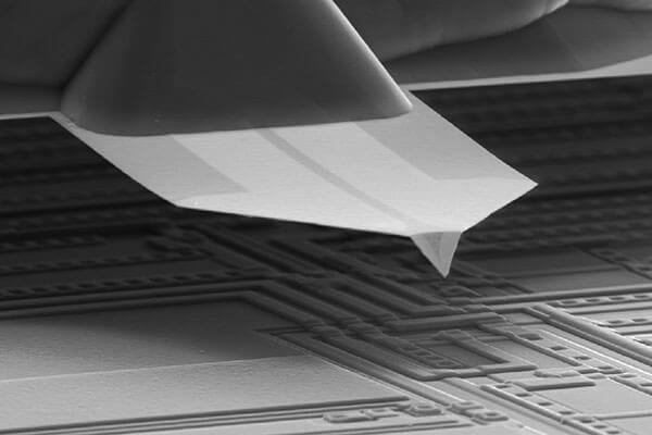
What is electron beam lithography?
Electron Beam Lithography Electron Beam Lithography is a specialized technique for creating extremely fine patterns. It is derived from the scanning electron microscope. Electron beams can be focused to a few nanometres in diameter. The basic idea behind electron beam lithography is identical to optical lithography.
What is vibrational spectroscopy?
29. Vibrational / Infrared Spectroscopy: Molecules and crystals can be thought of as systems of atoms or ions connected by springs (chemical bonds). These systems can be set into vibration, and vibrate with frequencies determined by the atomic weight and by bond strengths. They are at very high frequencies ranging from 10l2 to 1Ol4Hz, which is in the infrared (IR) regions of the electromagnetic spectrum. The oscillations combine with an impinging beam of infrared electromagnetic radiation and to exchange energy with it when the frequencies are in resonance. In the infrared experiment, the intensity of a beam of infrared radiation is measured before and after it interacts with the sample. The identities, atomic arrangements, and concentrations of the chemical bonds that are present in the sample can be determined. Optical Spectroscopy Cont.
What is UV lithography?
Photolithography, also termed optical lithography or UV lithography, is a process used in microfabrication to pattern parts of a thin film or the bulk of a substrate. It uses light to transfer a geometric pattern from a photomask to a light-sensitive chemical "photoresist", or simply "resist," on the substrate. A series of chemical treatments then either engraves the exposure pattern into, or enables deposition of a new material in the desired pattern upon, the material underneath the photo resist.
What is the purpose of electron beam lithography?
Electron-beam lithography (often abbreviated as e-beam lithography) is the practice of scanning a focused beam of electrons to draw custom shapes on a surface covered with an electron-sensitive film called a resist ("exposing").The electron beam changes the solubility of the resist, enabling selective removal of either the exposed or non-exposed regions of the resist by immersing it in a solvent ("developing").
What is the branch of nanotechnology that studies and applies nanometer-scale structures?
Nanolithography is the branch of nanotechnology concerned with the study and application of fabricating nanometer-scale structures, meaning patterns with at least one lateral dimension between 1 and 100 nm.
What is the name of the printing method based on oil and water?
Lithography (from Ancient Greek λίθος, lithos, meaning "stone", and γράφειν, graphein, meaning "to write") is a method of printing originally based on the immiscibility of oil and water. The printing is from a stone (lithographic limestone) or a metal plate with a smooth surface.
What is a nanometer?
A branch of nanotechnology in which standard size tools are used to manufacture simple structures and devices with dimensions on the order of a few nanometer s or less, where one nanometer (1 nm) is equal to a billionth of a meter (10 -9 m).
What is a photoresist?
A photoresist is a light-sensitive material used in several industrial processes, such as photolithography and photoengraving, to form a patterned coating on a surface.
