Metallization is the general process of adding a thin metal film of metals like aluminum to a product or material. Vacuum coating, contrarily, is one of the metalizing processes. Its working starts by evaporating a metal coating in a vacuum chamber.
What happens to the metal layer when the temperature rises?
What is the process of silyation?
What happens to the photoresist after etching?
What is reactive ion etching?
What is the process of forming a circuit?
What is the term for the evaporation of metals?
What metals are exposed to employees?
See 4 more
About this website

What is metallization reaction?
Metallization is a coating process of a metallic layer on a non-metallic substrate such as glass, ceramic or polymer.
What is use of metallization process in VLSI?
Metallization Process in which a thin layer of metal is formed which is used to make interconnections between the components on the chip as well as interconnections between the components and the outside world.
Why is metallization done?
Vacuum metalization is done for many reasons; aesthetically it adds a unique, eye catching appearance. Metallized substrates can have a highly reflective mirror like finish or be used in conjunction with other processes, like coating or laminating to create a decorative effect.
What is metallization in integrated circuit?
The metallizations on integrated circuits are the electrical conductors that connect the transistors and other components on the chip. At this time, aluminum is the most common metallization. To prevent electromigration, aluminum is generally alloyed with small quantities of copper and/or silicon.
Which is used for metallization?
What Materials Are Used in Metalizing? Metalizing systems are capable of spraying the following metals: aluminum, bronze, chrome, nickel, stainless steel, tungsten, and more. However, Zinc, Aluminum, and Zinc/Aluminum are the most common metals used in the metalizing process.
What is metallization for semiconductors?
After devices have been fabricated in the silicon substrate, connections must be made to link the circuits together. This process is called metallization. Metal layers are deposited on the wafer to form conductive pathways.
What are the types of metallization?
Metallization is deposited by either physical vapor deposition (PVD) or chemical vapor deposition (CVD). The most common forms of physical vapor deposition (PVD) are evaporation, e- beam evaporation, plasma spray deposition, and sputtering.
How do you calculate metallization?
Metallization is usually expressed as a percentage: Fe Metallic/Fe Total x 100. For example, a DRI pellet that has 86 % Fe Metallic and 92 % Fe Total would have 93 % Metallization.
What is metallization rate?
Metallization is the percentage of metallic Fe out of the total iron content. The rate of metallization depends on the DRI process and how it is operated, typically the higher the metallization rate, the lower the production rate and higher the specific consumptions rates for natural gas and electrical power.
What are the various problems occur in metallization?
Outgassing of the substrate. A leak in the vacuum system. Broken filaments in the metallizer. The basecoat is not completely cured and solvents are still escaping.
What is electro metallization?
Thermal spray processes are often referred to as metallizing. Metals applied in such a manner provide corrosion protection to steel for decades longer than paint alone. Zinc and aluminum are the most commonly used materials for metallizing steel structures.
What is metallization explain the physical Vapour deposition process for metallization?
Vacuum metallization (or physical vapor deposition) is a process in which the metal used for the application to the surface of the plastic (very often aluminum, although other metals are also used) is heated in a vacuum chamber and to its vaporization point, which is lower than the melting point of the plastic material ...
What are the types of metallization?
Metallization is deposited by either physical vapor deposition (PVD) or chemical vapor deposition (CVD). The most common forms of physical vapor deposition (PVD) are evaporation, e- beam evaporation, plasma spray deposition, and sputtering.
What are the various problems occur in metallization?
Outgassing of the substrate. A leak in the vacuum system. Broken filaments in the metallizer. The basecoat is not completely cured and solvents are still escaping.
What is metallization explain the physical Vapour deposition process for metallization?
Vacuum metallization (or physical vapor deposition) is a process in which the metal used for the application to the surface of the plastic (very often aluminum, although other metals are also used) is heated in a vacuum chamber and to its vaporization point, which is lower than the melting point of the plastic material ...
What are the desired properties of the metallization for the integrated circuits?
Metallization must have low resistivity for low power consumption and high integrated circuit speed, smooth surface for high resolution patterning process, high resistance to electro-migration to achieve high device reliability, and low film stress for good adhesion to underlying substrate.
Metallization: A Detailed Overview of the Metallization Process - WellPCB
Exposure of your products to harsh conditions, be it extreme weather or mechanical damage, can affect them. Therefore, having a suitable coating system can save your equipment in the long -term. There are two major coating systems, and that’s through galvanizing or metalizing. Generally, metallization is better, despite both of them being efficient.
Metallization Process | Types of Metallization | Applications
resistivity (μΩ-cm), melting point (°C), and; linear thermal expansion coefficient (ppm/ ° C) The resistivity ρ for the pure, thick and single crystalline film is lower ; while for impure and grain boundaries, it is higher.
Metalizing, Electric Arc, Flame Spray | A&A Thermal Spray Coating
Metalizing. Metalizing is a general name given to a thermal spray coating process that is used for coating metal on product surfaces. The resultant metallic coatings can be used for protective, decorative or functional purposes.
Metallisation - definition of metallisation by The Free Dictionary
Present Perfect Continuous; I have been metallizing: you have been metallizing: he/she/it has been metallizing: we have been metallizing: you have been metallizing
What Are the Various Metallization Processes?
In general, the metallization process entails preparing the surface via abrasive blasting to remove imperfections and defects, followed by the application of heat to produce molten particles that are sprayed onto the surface. Contact with the surface causes the particles to flatten out and freeze, which creates adhesion to the surface and between the individual particles.
What is metalization coating?
Metallization is a general term that refers to the application of a metal coating to another metallic or non-metallic surface. Depending on the desired result, the coating can consist of metals such as zinc, gold, aluminum or silver.
How does zinc react with iron?
The zinc reacts with the iron in the steel to form an alloy coating the provides excellent corrosion protection. Upon removal of the substrate from the zinc bath, the substrate then undergoes a draining or vibrating process to remove the excess zinc. Galvanization will continue after substrate removal until it cools.
Why are metallized coatings better than other coatings?
Increased durability — Most metallized coatings are known for their ability to adhere to the surface of the underlying workpiece or substrate. They are less likely to peel, blister, crack or flake than other types of finishes, which increases the substrate’s durability.
How is a metal vaporized?
Vacuum metallizing — This form of metallization involves boiling the coating metal in a specially designed vacuum chamber and then allowing the condensation to form a deposit on the substrate’s surface. The coating metal can be vaporized via techniques such as plasma or resistance heating.
What is Surtech metallization?
Surtech has offered exceptional metallization services since 1982. Our specialized metallizing processes work well for manufacturing applications that require durability and excellent corrosion protection. Contact us to learn more about the benefits of metallization and receive a free project quote today.
Why is metalizing plastic important?
Metallizing a plastic surface will enable it to transfer an electric current, which is a vital manufacturing step in the electronics industry. Greater weather resistance — The steel on outdoor structures is vulnerable to the impact of snow, rain, wind and sun over time.
What is interconnection metallization?
Interconnection metallization interconnects thousands of MOSFETs or bipolar devices using fine-line metal patterns. It is also same as gate metallization for MOSFET. All metallization directly in contact with semiconductor is called contact metallization. Polysilicon film is employed in the form of metallization used for gate and interconnection of MOS devices. Aluminium is used as the contact metal, on devices and as the second-level inter-connection to the outside world. Several new schemes for metallization have been suggested to produce ohmic contacts to a semiconductor. In several cases a multiple-layer structure involving a diffusion barrier has been recommended. Platinum silicide (PtSi) has been used as a Schottky barrier contact and also simply as an ohmic contact for deep junction. Titanium/platinum/gold or titanium/palladium/gold beam lead technology has been successful in providing high-reliability connection to the outside world. The applicability of any metallization scheme in VLSI depends on several requirements. However, the important requirements are the stability of the metallization throughout the IC fabrication process and its reliability during the actual use of the devices.
What is the final step in wafer processing?
Metallization is the final step in the wafer processing sequence. Metallization is the process by which the components of IC’s are interconnected by aluminium conductor. This process produces a thin-film metal layer that will serve as the required conductor pattern for the interconnection of the various components on the chip.
Why is an electron gun used for refractory metals?
Electron-gun cause radiation damage, but by heat treatment it can be annealed out. This method is advantageous because the evaporations take place at pressure considerably lower than sputtering pressure.
How is evaporation deposited?
In the evaporation method, which is the simplest, a film is deposited by the condensation of the vapour on the substrate. The substrate is maintained at a lower temperature than that of the vapour. All metals vaporize when heated to sufficiently high temperatures. Several methods of heating are employed to attain these temperatures. For AI deposition, resistive, inductive (RF), electron bombardment [electron-gun] or laser heating can be employed. For refractory metals, electron-gun is very common. Resistive heating provides low throughput. Electron-gun cause radiation damage, but by heat treatment it can be annealed out. This method is advantageous because the evaporations take place at pressure considerably lower than sputtering pressure. This makes the gas entrapment in the negligible. RF heating of the evaporating source could prove to be the best compromise in providing large throughput, clean environment, and minimal levels of radiation damage.
Why does aluminum have momentum?
It occurs because of the enhanced and directional mobility of atoms caused by the direct influence of the electric field and the collision of electrons with atoms, which leads to momentum transfer.
How to solve the problem of gold?
The problem is generally solved by using aluminium lead wires, or another metal system, in circuits that will be subjected so elevated temperatures. One method is to deposit gold over an under layer of chromium. The chromium acts as a diffusion barrier to the gold and also adheres well to both oxide and gold.
When a metal is deposited on the semiconductor, a good ohmic contact should be formed?
This is possible, if the deposition metal does not perturb device characteristics. Also die contact should be stable both electrically and mechanically.
What is metallization in wafer processing?
Metallization is the final step in the wafer processing sequence. Metallization is the process by which the components of IC’s are interconnected by aluminium conductor. This process produces a thin-film metal layer that will serve as the required conductor pattern for the interconnection of the various components on the chip. Another use of metallization is to produce metalized areas called bonding pads around the periphery of the chip to produce metalized areas for the bonding of wire leads from the package to the chip. The bonding wires are typically 25 micro meters diameter gold wires, and the bonding pads are usually made to be around 100×100 micro meters square to accommodate fully the flattened ends of the bonding wires and to allow for some registration errors in the placement of the wires on the pads.
What is the most commonly used material for metallization of most IC’s, discrete diodes,?
Aluminium. Aluminium (At) is the most commonly used material for the metallization of most IC’s, discrete diodes, and transistors. The film thickness is as about 1 micro meters and conductor widths of about 2 to 25 micro meters are commonly used. The use of aluminium offers the following advantages:
Why is an electron gun used for refractory metals?
Electron-gun cause radiation damage, but by heat treatment it can be annealed out. This method is advantageous because the evaporations take place at pressure considerably lower than sputtering pressure.
How is evaporation deposited?
In the evaporation method, which is the simplest, a film is deposited by the condensation of the vapour on the substrate. The substrate is maintained at a lower temperature than that of the vapour. All metals vaporize when heated to sufficiently high temperatures. Several methods of heating are employed to attain these temperatures. For AI deposition, resistive, inductive (RF), electron bombardment [electron-gun] or laser heating can be employed. For refractory metals, electron-gun is very common. Resistive heating provides low throughput. Electron-gun cause radiation damage, but by heat treatment it can be annealed out. This method is advantageous because the evaporations take place at pressure considerably lower than sputtering pressure. This makes the gas entrapment in the negligible. RF heating of the evaporating source could prove to be the best compromise in providing large throughput, clean environment, and minimal levels of radiation damage.
Why does aluminum have momentum?
It occurs because of the enhanced and directional mobility of atoms caused by the direct influence of the electric field and the collision of electrons with atoms, which leads to momentum transfer.
How to solve the problem of gold?
The problem is generally solved by using aluminium lead wires, or another metal system, in circuits that will be subjected so elevated temperatures. One method is to deposit gold over an under layer of chromium. The chromium acts as a diffusion barrier to the gold and also adheres well to both oxide and gold.
When a metal is deposited on the semiconductor, a good ohmic contact should be formed?
This is possible, if the deposition metal does not perturb device characteristics. Also die contact should be stable both electrically and mechanically.
What happens to the metal layer when the temperature rises?
As the temperature rises, the metal to be deposited is melted and wets the filament. The current through the filament is increased further, until the metal vaporizes. The metal vapor then condenses on the cooler surface of the semiconductor wafers, forming the desired metal layer. Electron-Beam Evaporation.
What is the process of silyation?
During silyation, silicon atoms are introduced into the surface of the organic resist. This process can be accomplished with either wet or dry procedures. Most commonly, a wet bath using either hexamethyldisilazane (HMDS) or silazone in xylene is used. The following are the potential hazards of silyation.
What happens to the photoresist after etching?
After etching, the remaining photoresist is stripped in a similar manner as during Device Fabrication.
What is reactive ion etching?
Reactive ion etching (RIE) is commonly used to etch metal layers . This process uses a combination of physical sputtering and chemically reactive species for etching at low pressures. RIE uses ion bombardment to achieve directional etching and a chemically reactive gas (carbon tetrafluoride, carbon tetrachloride, boron trichloride, and others) to maintain good etched layer selectivity. A wafer is placed into a chamber and given a negative electrical charge. The chamber is heated and brought to a low pressure, and then filled with a positively charged plasma of the reactive gas. The opposing electrical charges cause the rapidly moving plasma molecules to align themselves and strike the wafer surface vertically, thereby reacting with and volatizing the exposed metal layer. After etching, the remaining photoresist is stripped in a similar manner as during Device Fabrication.
What is the process of forming a circuit?
After devices have been fabricated in the silicon substrate, connections must be made to link the circuits together. This process is called metallization. Metal layers are deposited on the wafer to form conductive pathways. The most common metals include aluminum, nickel, chromium, gold, germanium, copper, silver, titanium, tungsten, platinum, and tantalum. Selected metal alloys may also be used. Metallization is often accomplished with a vacuum deposition technique. The most common deposition processes include filament evaporation, electron-beam evaporation, flash evaporation, induction evaporation, and sputtering.
What is the term for the evaporation of metals?
Electron-Beam Evaporation. Electron-beam evaporation, frequently called "e-beam, " uses a focused beam of electrons to heat the metal for deposition. The metal is kept in a water-cooled crucible and exposed to the electron beam, causing it to vaporize and condense on the wafers. Flash Evaporation.
What metals are exposed to employees?
Possible employee exposure to various metals, aluminum being the most common.
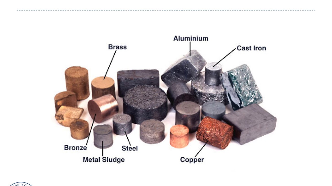
Aluminium
Metallization Application in VLSI
- For VLSI, metallization applications can be divided into three groups: 1. Gates for MOSFET 2. Contacts, and 3. Interconnects. Interconnection metallization interconnects thousands of MOSFETs or bipolar devices using fine-line metal patterns. It is also same as gate metallization for MOSFET. All metallization directly in contact with semiconductor is called contact metallizati…
Ohmic Contacts
- When a metal is deposited on the semiconductor a good ohmic contact should be formed. This is possible, if the deposition metal does not perturb device characteristics. Also die contact should be stable both electrically and mechanically. Other important application of metallization is the top-level metal that provides a connection to the outside world. To reduce interconnection resist…
Metallization Processes
- Metallisation process can be classified info two types: 1. CVD and 2. Physical Vapour Deposition To know about CVD click on the link below. TAKE A LOOK : CHEMICAL VAPOUR DEPOSITION (CVD) CVD offers three important advantages. They are 1. Excellent step coverage 2. Large throughput 3. Low-temperature processing 4. The basic physical vapour depositio...
Deposition Methods
- In the evaporation method, which is the simplest, a film is deposited by the condensation of the vapour on the substrate. The substrate is maintained at a lower temperature than that of the vapour. All metals vaporize when heated to sufficiently high temperatures. Several methods of heating are employed to attain these temperatures. For AI deposition, resistive, inductive (RF), el…
Deposition Apparatus
- The metallization is usually done in vacuum chambers. A mechanical pump can reduce the pressure to about 10 to 0.1 Pa. Such pressure may be sufficient for LPCVD. An oil-diffusion pump can bring the pressure down to 10-5 Pa and with the help of a liquid nitrogen trap as low as 10-7 Pa. A turbomolecular pump, can bring the pressure down to 10-8-10-9Pa. Such pumps are oil-fre…
Metallization Patterning
- Once the thin-film metallization has been done the film must be patterned to produce the required interconnection and bonding pad configuration. This is done by a photolithographic process of the same type that is used for producing patterns in Si02 layers. Aluminium can be etched by a number of acid and base solutions including HCl, H3PO4, KOH, and NaOH. The most commonly …
Lift-Off Process
- The lift-off process is an alternative metallization patterning technique. In this process a positive photoresist is spun on the wafer and patterned using the standard photolithographic process. Then the metallization thin film is deposited on top of the remaining photoresist. The wafers are then immersed in suitable solvent such as acetone and at the same time subjected to ultrasoni…
Pattering For VLSI Applications
- VLSI applications require anisotropic etching techniques for metallization patterning because of the requirements of tight control on metallization dimensions. Therefore dry-etching techniques are most suitable. Reactive-ion etching (RIE) is anisotropic. Hence it is preferred. For RIE, reactive gases such as, Cl2 and CCI3F are used, hence the name reactive ion etching.