In this article, we discuss metastability, setup time, and hold time when designing a digital VLSI circuit. Critical Path, Throughput, and Latency The critical path is the longest path in the circuit and limits the clock speed. When describing a digital circuit there are two other important factors: latency and throughput.
What is a hold critical path?
Hold timing critical paths: As is quite obvious, those paths for which meeting hold timing is difficult, are hold critical paths. These paths may require many buffers to meet hold slack equation. Sometimes, we may encounter some timing paths which are violating in both setup and hold.
What is critical path analysis?
Critical path analysis, also known as "critical path planning," is a project management system that evaluates the duration of different tasks and identifies the fastest way to complete a job.
What are the different types of timing critical paths?
They can be divided into setup and hold timing critical paths. Setup timing critical paths: Those paths for which meeting setup timing is difficult, can be termed as setup critical timing paths. For these paths, the setup slack value is very close to zero and for the most part of design cycle, remains below zero.
What is the difference between critical path and noncritical path?
The duration of the critical path is the shortest possible time that one can complete the project. Noncritical paths, which are comprised of one or more tasks that are not dependent on the string of jobs in the critical path.

What is critical path in logic circuits?
The critical path is defined as the path between an input and an output with the maximum delay. Once the circuit timing has been computed by one of the techniques listed below, the critical path can easily be found by using a traceback method.
What is timing analysis in VLSI?
Static timing analysis (STA) is a way of evaluating a design's timing performance by testing for timing violations along all conceivable paths. Dynamic simulation, which determines the whole behaviour of the circuit for a given set of input stimulus vectors, is another technique to do timing analysis.
What is throughput in digital design?
Definition: The throughput of a digital system is the rate at which it computes outputs from new inputs. The throughput of a system is the rate at which it accepts inputs, or, equivalently, the rate at which it produces outputs.
What is VLSI microprocessor based?
Very large-scale integration is a process of embedding or integrating hundreds of thousands of transistors onto a singular silicon semiconductor microchip. VLSI technology's conception dates back to the late 1970s when advanced level processor (computer) microchips were also in their development stages.
What is skew in VLSI?
It's a difference between the clock arrival time across the chip. It's the time delta between the actual and expected arrival time of a clock signal. Clock skew is the timing differences between signals in a clock distribution system. Variation of arrival of clock at destination points in the clock Network.
What is clock gating in VLSI?
Clock gating is a power-saving feature in semiconductor microelectronics that enables switching off circuits. Many electronic devices use clock gating to turn off buses, controllers, bridges and parts of processors, to reduce dynamic power consumption.
What is latency in VLSI?
Latency is the time needed for an input change to produce an output change; latency can be expressed as a length of time or, in synchronous circuits, as a certain number of clock cycles.
What is difference between latency and throughput?
In other words: throughput is the number of data packets being successfully sent per second, and latency is the actual time those packets are taking to get there. So, the terms are related - they both relate to data transfer and speed.
What is difference between bandwidth and throughput?
Bandwidth and throughput both indicate network performance. The terms are often used together, but bandwidth refers to capacity, while throughput details how much data actually transmits. Bandwidth and throughput are two terms related to network performance.
What are the 5 levels in VLSI design?
Abstraction levels:Physical level : Rectangles, design rules.Circuit level : Transistors, R and C, analog voltage/current values.Logic level : Boolean logic gates, binary valued logic.Register Transfer Level : Adders, datapaths, binary valued words.Functional level : Processors, programs and data structures.
What transistor is used in VLSI?
MOS technology is considered as one of the very important and promising technologies in the VLSI design process. The circuit designs are realized based on pMOS, nMOS, CMOS and BiCMOS devices. The pMOS devices are based on the p-channel MOS transistors.
How many types of VLSI are there?
VLSI Design is divided into two major groups as programmable design and nonprogrammable designs.
What is timing analysis in digital circuits?
Timing analysis is the methodical analysis of a digital circuit to determine if the timing constraints imposed by components or interfaces are met. Typically, this means that you are trying to prove that all set-up, hold, and pulse-width times are being met.
Why is timing important in VLSI?
During designing there is a trade-offs between speed, area, power, and runtime according to the constraints set by the designer. However, a chip must meet the timing constraints to operate at the intended clock rate, so timing is the most important design constraint.
What are timing constraints in VLSI?
Timing constraints are used to specify the timing characteristics of the design. Timing constraints may affect all internal timing interconnections, delays through logic and LUTs and between flip-flops or registers. Timing constraints can be either global or path-specific.
What is timing violation in VLSI?
If M > Tclk – S , it results into timing violation, called as Setup violation. This means, that the combinational logic delay is very large and hence data change is very slow. To satisfy the 'setup' requirement, the combinational logic delay should be decreased.
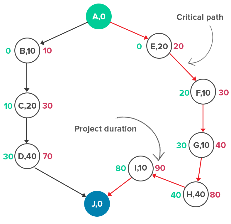
What is critical path?
When describing a digital circuit there are two other important factors: latency and throughput. Latency is the time needed for an input change to produce an output change; latency can be expressed as a length of time or, in synchronous circuits, as a certain number of clock cycles. Throughput refers to the rate at which data can be processed.
Why does the clock speed decrease in VLSI?
In such cases, our clock speed will decrease to ensure that the delays associated with the critical path do not lead to setup-time violations. Pipelining is a technique whereby we divide a combinational path into multiple parts and include a register at the end of each partial path. In this way, we divide the critical path into multiple small paths, and this allows us to increase the clock speed and, consequently, the throughput of the circuit.
What is combinational logic?
Combinational logic refers to a circuit that computes an output based only on the current input signals.
What is the hazard of a logic low state?
Assume we are in the (1,1,1) input state and the output is steady at 1. If b changes from 1 to zero the output of the lower AND gate will transition before that of the upper AND gate, resulting in a temporary logic low on the output. This logic-low state is invalid, because a (1,0,1) input pattern should produce a logic-high output. This brief invalid output state is referred to as a hazard.
Can a pipelined path increase clock speed?
However, the divided and pipelined path (see Figure 5) contains shorter combinational paths, and this means we can increase the clock speed. However, as a trade-off, the latency of the path will increase.
What is critical path?
Critical paths, which are the series of dependent tasks with the longest duration that must be completed in a specific sequential order. The duration of the critical path is the shortest possible time that one can complete the project.
What is critical path analysis?
Critical path analysis, also known as "critical path planning," is a project management system that evaluates the duration of different tasks and identifies the fastest way to complete a job.
Why do critical path tasks have no float?
Tasks on the critical path have no float because they are dependently connected. Critical path analysis requires constant attention to the duration of each task so you know which path is most important. Changing the allocation of resources to speed up a task may cause that path to become noncritical.
Why is critical path analysis important in project management?
Critical path analysis streamlines project management for complex jobs with many sequential tasks.
Why do we need a critical path chart?
Once you have adequately outlined your project, you can create a critical path chart to make it easier to visualize the flow of activity. There are two primary options for charting critical path analysis.
What is program evaluation and review technique diagram?
Program Evaluation and Review Technique diagrams clearly show all sequential and parallel tasks and their connections to one another. This diagram features each task in a circle. Arrows between these circles connect tasks with their predecessors. Using arrows simplifies critical path analysis and network planning by clearly identifying where parallel paths merge.
What is timing critical path?
Those timing paths, which are very hard to meet in timing are called timing critical paths. They can be divided into setup and hold timing critical paths. Setup timing critical paths: Those paths for which meeting setup timing is difficult, can be termed as setup critical timing paths. For these paths, the setup slack value is very close ...
What is the worst case for combinational delay?
In other words, worst case combinational delay is 200 ps (2 times scaling).
Is hold timing critical?
Hold timing critical paths: As is quite obvious , those paths for which meeting hold timing is difficult, are hold critical paths. These paths may require many buffers to meet hold slack equation. Sometimes, we may encounter some timing paths which are violating in both setup and hold. There is not enough setup slack to make them hold timing clean ...
Can setup and hold be negative?
Thus, for the same timing path, both setup and hold slacks are coming out to be negative. For this path, we cannot meet both setup and hold provided all these conditions. One of the solutions could be to use cells with less delay variability. Or we can limit the operating conditions to a tighter range, for instance, 1.15 to 1.25 V instead. This will improve both setup and hold slack values. If this is not an option, the only option left to satisfy timing is to add delay elements to bring hold slack to zero and reduce the frequency as the inherent variations of cells will not allow the path to operate beyond a certain frequency. Let us check at what maximum frequency our timing path will work.
Critical Path, Throughput, and Latency
Flip-Flops and Combinational Logic
- A digital circuit can consist of sequential logic and combinational logic. Sequential logic refers to circuits whose output depends on previous states. In other words, it involves memory that stores previous states and allows a decision to be made based on these previous states and the current input signals. In the digital realm, flip-flops are the standard devices used for storing previous lo…
Setup Time
- A digital circuit designed for FPGA or ASIC purposes needs combinational logic for calculations. We usually build multipliers, subtractors, adders, etc., with logic gates. For storing input and output values for these combinational logic circuits, we use flip-flops. Flip-flops are at the beginning and at the end of all critical paths, as shown in Figure 3. To avoid a setup-time violatio…
Pipelining
- In VLSI designs, we may face a very long critical path due to an extensive combinational circuit. In such cases, our clock speed will decrease to ensure that the delays associated with the critical path do not lead to setup-time violations. Pipelining is a technique whereby we divide a combinational path into multiple parts and include a register a...
Hold Time
- The input to a flip-flop should be stable for an amount of time equal to or greater than the hold time. For example, in Figure 6, assume the delay of the combinational path between FF1 and FF2 is 0.7ns, the flip-flop setup time is 2ns, and its hold time is 1ns. If we assume that the propagation delay of the flip-flops is zero, after a clock edge the output of FF1 will change immediately, and 0…
Clock-Crossing
- In most modern designs, multiple clock frequencies are used. ADCs or DACs may have a clock that is not synchronized with the FPGA clock, and yet the ADC or DAC signals must be introduced into the FPGA clock domain. When we're working with multiple clock domains, we need to be careful to avoid situations that could lead to metastability. We will need to achieve synchronizati…
Conclusion
- In this article, we talked about hold-time violations and how to avoid them by adding a delay to fast logic paths. We also explained setup-time violations and we discussed pipelining as a method of avoiding timing problems in circuits that include a long critical path. Finally, we introduced the idea of multiple clock domains, and we looked at a simple Verilog approach t…