What is SWD in arm?
ARM's S erial W ire D ebug (SWD) replaces the traditional 5-pin JTAG debug interface by introducing a 2-pin interface with a clock (SWDCLK) and a single bi-directional data pin (SWDIO), providing all the normal JTAG debug and test functionality, anyhow dayisy-chaining devices as via JTAG is not possible.
What is SWD (Serial Wire Debug)?
SWD stands for Serial Wire Debug is the protocol designed by ARM for programming and debugging their microcontrollers. Since SWD specializes in programming and debugging, it comes with many special features that is usually not available anywhere else like sending debug info to the computer via the IO line.
How many pins does SWD protocol have?
SWD protocol has only 2 pins namely SWDIO (Serial Wire Data Input Output: the data line) and SWCLK (Serial Wire Clock: the clock line) SWD supports star topology in terms of architecture.
What is SW-DP port used for?
Serial Wire Debug Port (SW-DP). This port uses the SWD protocol to access the DAP. Serial Wire / JTAG Debug Port (SWJ-DP). This port can use either JTAG or SWD to access the DAP. This is a common interface found on many microcontrollers. It reuses the TMS and TCK JTAG signals to transfer the SWDIO and SWDCLK signals respectively.
What is SWD communication?
Serial Wire Debug (SWD) is a 2-pin (SWDIO/SWCLK) electrical alternative JTAG interface that has the same JTAG protocol on top. SWD uses an ARM CPU standard bi-directional wire protocol, defined in the ARM Debug Interface v5.
What are the SWD signals?
Serial Wire Debug (SWD) is commonly used on reduced pin-count target devices. SWD only requires two pins, instead of the four pins used by JTAG.
What is SWD in microcontroller?
Serial Wire Debug (SWD) is really just a modification/implementation of JTAG specifically for ARM processors. SWD puts the 2 pins (SWDIO and SWCLK) on top of the JTAG pins allowing a user to use either JTAG or SWD without the need to breakout more pins.
What is the difference between JTAG and SWD?
SWD is an ARM specific protocol designed specifically for micro debugging. JTAG (Joint Test Action Group) was designed largely for chip and board testing. It is used for boundary scans, checking faults in chips/boards in production.
How many pins are required for SWD?
two pinsIn SWD mode, two pins are used for debugging: one bi-directional pin (SWDIO) transfers the information and the second pin (SWDCLK) clocks the data. A third pin (SWO) delivers the trace data at minimum system cost.
What is SWD programmer?
SWD, also known as Serial Wire Debug is a 2-pin interface (SWDIO/SWCLK) of which it's also an alternative JTAG interface that has the same JTAG protocol. SWD uses an ARM CPU standard bi-directional wire protocol, defined in the ARM Debug programmer.
What is SWD embedded system?
SWD stands for Serial Wire Debug is the protocol designed by ARM for programming and debugging their microcontrollers. Since SWD specializes in programming and debugging, it comes with many special features that is usually not available anywhere else like sending debug info to the computer via the IO line.
What JTAG means?
Joint Test Action GroupThe Joint Test Action Group, or JTAG, is the name given for the IEEE 1149.1 Standard Test Access Port and Boundary-Scan Architecture. This architecture is used in most computer processors since Intel released the first processor with JTAG, the 80486.
What is JTAG connector?
A JTAG interface is a special interface added to a chip. Depending on the version of JTAG, two, four, or five pins are added. The four and five pin interfaces are designed so that multiple chips on a board can have their JTAG lines daisy-chained together if specific conditions are met.
Is JTAG still relevant?
For embedded developers and hardware hackers, JTAG is the de facto standard for debugging and accessing microprocessor registers. This protocol has been in use for many years and is still in use today.
How do I use a JTAG programmer?
1:032:01USB JTAG PROGRAMMER DEMO - YouTubeYouTubeStart of suggested clipEnd of suggested clipI'm just connecting the board with programmer so just connector now I open an FPGA program or to theMoreI'm just connecting the board with programmer so just connector now I open an FPGA program or to the PC.
What is SWD CLK?
ARM's Serial Wire Debug (SWD) replaces the traditional 5-pin JTAG debug interface by introducing a 2-pin interface with a clock (SWDCLK) and a single bi-directional data pin (SWDIO), providing all the normal JTAG debug and test functionality, anyhow dayisy-chaining devices as via JTAG is not possible.
What are JTAG pins?
A JTAG interface is a special interface added to a chip. Depending on the version of JTAG, two, four, or five pins are added. The four and five pin interfaces are designed so that multiple chips on a board can have their JTAG lines daisy-chained together if specific conditions are met.
What is serial wire output?
Serial Wire Output (SWO) alongside Serial Wire Debug (SWD) allows for the CPU to emit real-time trace data. In particular, when used with an Instrumentation Trace Macrocell (ITM), it can be used to form a Serial Wire Viewer (SWV). The ITM ports are provided by the ARM controller.
What is JTAG debugger?
Today JTAG is used as the primary means of accessing sub-blocks of integrated circuits, making it an essential mechanism for debugging embedded systems which might not have any other debug-capable communications channel.
What is SWCLK and SWDIO?
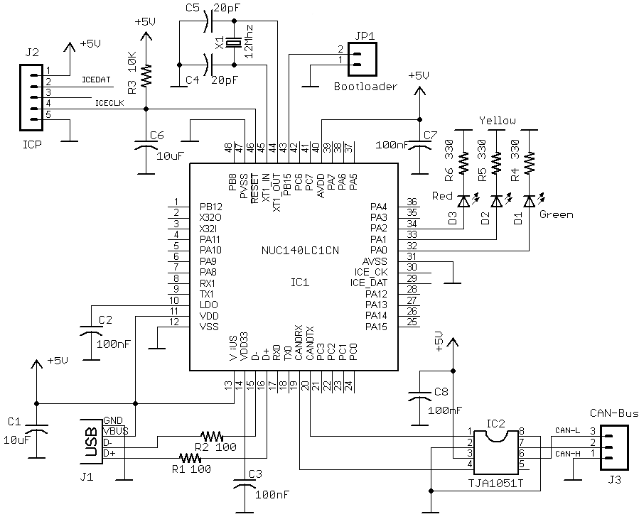
SWDIO and SWCLK are overlaid on the TMS and TCK pins, allowing to use the same connector for JTAG and SWD. In order to communicate with a device via SWD, data is send on SWDIO, synchronous to the SWCLK. With every rising edge of SWCLK, one bit of data is transmitted or received on the SWDIO pin.
What is SWDIO in ARM?
ARM's S erial W ire D ebug (SWD) replaces the traditional 5-pin JTAG debug interface by introducing a 2-pin interface with a clock (SWDCLK) and a single bi-directional data pin (SWDIO), providing all the normal JTAG debug and test functionality, anyhow dayisy-chaining devices as via JTAG is not possible. SWDIO and SWCLK are overlaid on the TMS and TCK pins, allowing to use the same connector for JTAG and SWD. In order to communicate with a device via SWD, data is send on SWDIO, synchronous to the SWCLK. With every rising edge of SWCLK, one bit of data is transmitted or received on the SWDIO pin.
What is serial wire output?
Serial wire output, allowing the CPU to output custom data like printf output, asynchronous to SWCLK and other debug pins. Usually shared with the TDO pin on devices which support JTAG and SWD. Not available on all devices which support SWD.
What does SWD support?
SWD supports star topology in terms of architecture.
What does SWD mean in ARM?
SWD stands for Serial Wire Debug is the protocol designed by ARM for programming and debugging their microcontrollers. Since SWD specializes in programming and debugging, it comes with many special features that is usually not available anywhere else like sending debug info to the computer via the IO line.
What was the debugging world before SWD?
Earlier before the advent of protocols like SWD and JTAG the debugging world was just full of chaos. Each major manufacturer came up with their own proprietary way of loading the code onto their microcontrollers and as a result the only ones who had to suffer were people like us the embedded engineers. Each time a big manufacturer releases a microcontroller, we, the embedded engineers, need to learn about their proprietary protocols for loading code into our microcontrollers.
Is SWD as ubiquitous as ARM?
Since ARM’s business model is just licensing its designs a lot of manufacturers make debug adapters based on SWD designs and this makes SWD as ubiquitous as ARM-based chips themselves!
When did the IEEE 1149.1 protocol come out?
The protocol they came up with was documented into IEEE 1149.1 in 1990. Later this document was revised and made better and at the time of this writing the latest standard was IEEE 1149.7.
Can all microcontrollers use the same debug protocol?
This way all of the microcontroller manufacturers can all implement the same debugging protocol so that the same debug adapter can be used with all of the microcontrollers that implement the given standard!
How many signals does SWD use?
As said earlier, SWD uses only two signals :
How long does it take to run SWD?
The operation takes less than two seconds, and reliably discovered SWD interfaces on all the tested boards so far.
What is the bus used in SWD?
Contrary to JTAG, which chains TAPs together, SWD uses a bus called DAP (Debug Access Port). On this DAP, there is one master (the DP – Debug Port) and one or more slaves ( AP – Access Ports), similar to JTAG TAPs. The DP communicates with the APs using packets that contain the AP address.
What is JTAG protocol?
For embedded developers and hardware hackers, JTAG is the de facto standard for debugging and accessing microprocessor registers. This protocol has been in use for many years and is still in use today. Its main drawback is that it uses a lot of signals to work (at least 4 – TCK, TMS, TDI, TDO). This has become a problem now ...
What is the protocol used to connect to the DAP?
To sum this up, an external debugger connects to the DAP via the DP using a protocol called SWD. This whitepaper from ARM shows a nice overview of the SWD architecture :
How many bits is a JTAG to SWD?
2. Send the 16-bit JTAG-to-SWD select sequence on SWDIOTMS.
Is the DAP fully accessible?
Now that the debug power domain is up, the DAP is fully accessible. As a first discovery process, we will query an AP, then scan for all APs in the DAP.
What is SWD in ARM?
SWD, also known as Serial Wire Debug is a 2-pin interface (SWDIO/SWCLK) of which it's also an alternative JTAG interface that has the same JTAG protocol. SWD uses an ARM CPU standard bi-directional wire protocol, defined in the ARM Debug programmer.
Where are the SWD pads on a Wio terminal?
For Wio Terminal, the SWD interface pads are on the bottom of the front side of Wio Terminal (Bare PCBA without casing). There are three jumper wires that need to be led out:
What is SWD in flash?
All transactions performed via SWD, including programming to on-chip flash, are converted into read and/or write operations. Each operation in the following text has a corresponding function in the reference implementation source code, as will be highlighted.
What register is used for SWD?
This read actually passes through the SW-DP RDBUFF register, and so this operation actually uses a read SW-DP register operation.
What is a 3 bit acknowledgement in SW-DP?
Every access by a debugger to a SW-DP starts with an operation request. Whenever a debugger issues an operation request to a SW-DP, it expects to receive a 3-bit Acknowledgement . The next table summarizes how the debugger must respond to this acknowledgement, for all possible cases.
What happens if SW-DP is not able to process the request from the debugger immediately?
If the SW-DP is not able to process the request from the debugger immediately it must issue a WAIT response. However, a WAIT response must not be issued to the following DP register accesses. In these cases, the DP must always process these three requests immediately:
What is serial interface SW-DP?
The serial interface to the SW-DP must use a connection sequence, to ensure that hot-plugging the serial connection does not result in unintentional transfers. The connection sequence ensures that the SW-DP is synchronized correctly to the header that is used to signal a connection. It consists of a sequence of 50 clock cycles with data = 1, that is, with the serial data signal asserted HIGH by the debugger. This connection sequence is also used as a line reset sequence. The protocol requires that any run of 50 consecutive 1s on the data input is detected as a line reset, regardless of the state of the protocol.
How to invoke IAP?
To invoke an IAP command the execution context of the IAP procedures must be prepared, including writing of the parameters and return address into core registers, and write data to program in SRAM. To avoid any interference from code already running in the target system the core must first be prevented from continuing execution, in other words it must be halted. Once the IAP command context is setup, the core execution is resumed. It is also necessary to know when the IAP has completed the programming operation, so a BKPT instruction needs to be placed at the IAP return address to halt the core as soon as IAP function completes. The status of the core can be polled to wait until this sequence of events has completed.
What is a DAP and AP?
This is the combination of DP and AP; in others words, references to “DAP” imply “The DP and The AP”. DP and AP have dedicated bus to communicate with each other; DPs can select an AP (when there are multiple APs) and the register to access in that AP. All transactions are initiated by DPs, and reads/writes to AP registers are performed by DPs.
What is serial wire debug?
Serial Wire Debug (SWD) is a two-wire protocol for accessing the ARM debug interface. It is part ofthe ARM Debug Interface Specification v5 and is an alternative to JTAG. The physical layer of SWDconsists of two lines:
What is the SWO pin on an EFM32?
The EFM32 has three pins used for debugging. Two of them are the SWDIO and SWCLK pins usedby SWD. The last pin is called Serial Wire Output (SWO) and is used for debugging output. SWO isan asynchronous, one-directional protocol used by the internal debug components in the core to outputvarious debug information. This pin is not required to program the device.
What is SWO in ARM?
SWO specifies a dedicated pin, in addition to the debug signals of the SWD interface, which allows the target CPU to output specific data like printf output on a dedicated pin via UART or Manchester protocol. This pin is unidirectional, so it is not possible to send data to the target CPU on this pin.
Does SWO follow CPU clock?
On some target devices however the SWO clock does not follow the CPU clock directly, but e.g. has an own static clock source or similar. To still be able to use SWO in such setup the debugger must know the "new" actual clock source. So either set the static clock source as the SWO clock speed in the configuration of the SWO software tool you are using, or you can use a JLinkScript for this with function SWO_GetSWOBaseClock.